
For most startups and developers, working with nanomaterials is out of the question because of the cost involved. Today, if you wanted to build things in the nanometer scale, you’d think of a silicon company such as Intel or TSMC. Although they may have perfected chip design at 7nm or 5nm process, you cannot scale their design principles to large area applications.
For example, consider an ultra-thin car window. The foundry costs of nanoscaling a 4 x 4 cm silicon chip to 2′ x 2′ dimensions can run into tens of thousands of dollars. This is also pretty illogical because the car isn’t probably going to be worth that much. With present fabrication standards in sheet design, at best you can achieve an ultra-thin automotive window 0.1mm to 0.5mm thick.
Where the limitations of foundry technology begin, the field of nano-optics can offer a way out. A Nova Scotia, Canada-based company called Metamaterial Inc. (META) has invented a groundbreaking solution to produce large-area nano-patterning at affordable costs. Their applications include rollable touchscreen displays, solar panels, 5G antennas, and smart eyewear for AR/VR.
We spoke to George Palikaras, the founding President and CEO of Metamaterial who shared with us his company’s vision of solving fundamental physics problems in dealing with nanoscale fabrication.
What Are Metamaterials?
There are many visual examples of nanoeffects in ancient arts, such as the famous ancient Damascus sabre which offered beautiful patterning due to the presence of carbon nanotubes. In the medieval ages, large-scale stained-glass windows for churches were a common sight. The concept of metamaterials (“meta” means beyond) simply takes the idea of random nanoparticles to an organized level.

Accordingly in physics, metamaterials refer to a class of composite materials which can control light at a nano-scale to enhance connectivity, absorption, reflection, and the bending of light at certain angles.
One of the properties of metamaterials is that they exhibit a negative index of refraction. It’s a kind of electromagnetic cloaking in naturally occurring materials, which can impact light on a macroscopic scale to greatly increase permeability and permittivity of light. It is possible to use this property of light to play around with the shape of objects, to make them flatter and ultra-thin to a nanometer scale.

Says George: “The smartness comes in when the thickness and size of nano-scale objects you create (also called “nanowires”) determine the color of the spectrum and you’re able to fashion very advanced materials. At Metamaterial, our scientists have worked at selecting the right materials from a library of materials including silicon, metals, and many other objects. The likes of Intel did something similar with semiconductor chip design, and right now we’re pushing for the same boundaries in the field of optics.”
Indeed, such a scale of thickness in nanometers can drastically reduce the cost of macro applications, such as solar panels ranging several kilometers, something not possible with conventional foundry technology. George considers the approach of Metamaterial to design as a democratizing mission, which he believes will make low-cost nanopatterning available to one and all.
What Are the IoT Applications of Metamaterials?
Compared to any other smart materials or other composite objects, metamaterials can push the boundaries in fabrication, making things 100 times thinner. This makes them a candidate of choice for making bulk materials for cheap and readily available off the shelf. The metamaterials by this company were used to make bendable phones, which have become quite a sensation in recent years, and they were already covered on this.
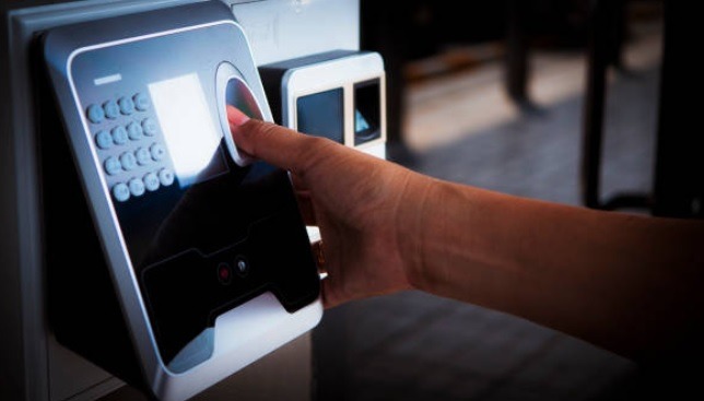
One of the metamaterial applications mentioned by George is in collaboration with Samsung’s Advanced Institute of Technology team. They have come up with fingerprint sensors for next-generation smartphones and tablets. For that, they use Metamaterial’s Rolling Mask Lithography® technology, which is free from form-factor limitations to produce functional surfaces. This is a drastic improvement over Indium Tin Oxide (ITO), which is currently used to shine the displays of smartphones.
Metamaterials can have up to 99 percent transparency and a high conductivity in the range of 1-2 Ω/square. This makes them a natural fit for any touchscreens that go underneath them. Adds George: “When you decouple the shape (of objects) from their function, you can achieve so much more with sheet design. You can stack them together for row-to-row printing like the newspaper reels of older times. That is the kind of future we are building with metamaterials.“
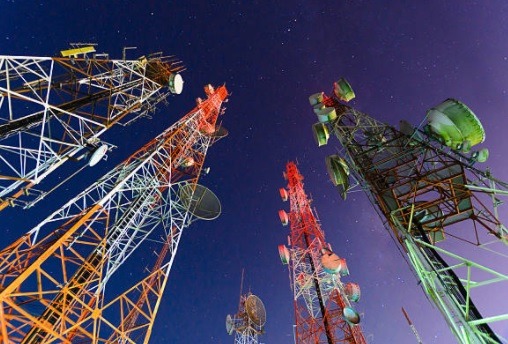
According to George, some of the other applications of metamaterials include designing solar panels with up to 75 percent less thickness without losing the efficiency of their solar cells. They are also working in the area of transparent antennas to improve 5G reception. George believes that the metamaterial-based transparent antennas can have a “repeater” effect on 5G signaling capabilities, overcoming most 5G limitations. This has applications in autonomous vehicles running on 5G networks.
Final Thoughts
A leading global business publication, Financial Times, has listed metamaterials (as well as George’s eponymous company named Metamaterial) as one of the 50 ideas that will change the world. From invisible cloaks to microwaves to satellite antennas and advanced acoustics and superlenses, metamaterials are expected to dominate IoT material design in the future. With several patents granted, Metamaterial seems to be on an Edison-esque mission to revolutionize the smart materials space.
So what is in it for developers? George assures us that Metamaterial has an open-source focus for developers working with Raspberry Pi and other boards wanting to bring the next innovation to market. They can access the ultra-thin metamaterial goods for their projects on an e-commerce site, adding that the prices they get for nanometer displays are much cheaper than what could be done in a foundry.
Get the best of IoT Tech Trends delivered right to your inbox!


